Computer vision and project mapping enable AR PCB debugging bliss
Imagine if you could identify a component and its schematic label by simply touching that component on your PCB. Imagine if you selected a pin in KiCAD and it started glowing on your real, physical PCB so you can find it easily. Imagine if you could see through your PCB’s solder mask to view the traces underneath. All of those things — and much more — are possible with this Augmented Reality Debugging Workbench (ARDW) system.
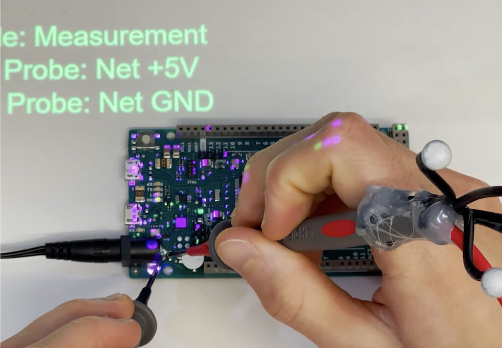
ARDW pairs tracking camera computer vision with projection mapping for fantastic augmented reality examination of PCBs. Touch a component with the special probes and ARDW will project the component’s name and label onto the table next to your board. Select a component or a component’s pin in KicAD and ARDW will project a highlighted overlay on the physical board showing you where it is. ARDW can even guide you through automated debugging by highlighting probe points and checking your measurements as you take them.
The team that developed ARDW demonstrated the system using Arduino Uno and Arduino Due boards, which were ideal choices because they’re open source and schematics are readily available. But ARDW can work with any PCB for which the user possesses design files.
It works with a plugin for KiCAD, which is open source PCB design software popular in the maker community and industry. Through KiCAD, ARDW gains access to the PCB layout and the schematics. It matches those up with the physical board sitting on the workbench and then projects graphics according to the selection and the board’s location. ARDW is extremely useful for all kinds of development, debugging, and quality control tasks.